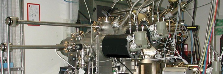

The HMMBE (High Mobility Molecular Beam Epitaxy) lab is a facility for the synthesis of high quality band-engineered compound semiconductor systems and devices
The High Mobility Molecular Beam Epitaxy is a facility dedicated to the growth of high purity III/V semiconductors in ultra-high vacuum with atomic layer control on compositions and thicknesses.
The model is a Veeco Gen II machine with a dedicated design for high mobility, equipped with As (2X), Ga (2X), Al, In effusion cells and Si and C doping sources for growth on 2” GaAs wafers. Grown structures range from high mobility two-dimensional electron systems in GaAs/AlGaAs (with mobilities up to the 107cm2/Vs range) and metamorphic In0.75Ga0.25As/ In0.75Al0.25As heterostructures (with mobilities up to the 5X105 cm2/Vs), to photonic structures and self-assembled nanostructures. A multi-wavelength optical process monitor allows accurate real-time control of substrate temperature and growth rate with <1% accuracy through interference measurements.The facility is completed by a variable temperature Oxford MagLab 2000 magneto transport equipment for electrical characterization (T in the 1.5 –400 K range,magnetic field up to 7 T), allowing classical and quantum Hall effect measurements to determine carrier density and mobility.
Instrumentation:A customized silicon source based on direct heating of a Si stripe by DC current has been developed in collaboration with the IOM technical services.A collaboration with Elettra is aimed at the development of X-ray photon beam detectors based on GaAs avalanche photodiodes which, if successful, will find wide application in new generation light sources.
Software: The control software of the MBE machine has been developed in house on a LabView platform, allowing flexibility in adding/adapting new sources and equipment. The acquisition software for the magnetotransport experiments been developed in house on a LabView platform as well.
The activity of the group is based on the development of high purity III/V semiconductors, with areas of application ranging from coherent transport o nanophotonics, spintronics and detectors. An activity concerns the development of GaAs/AlGaAs multiple QW systems for applications in Mid-IR quantum cavity electrodynamics. This allows the manipulation of light-matter interactions through strong coupling between photonic density of states and QW intersubband excitonic transitions giving rise to cavity polaritons. Applications range from fundamental studies of condensation phenomena in electronic systems, to ultrafast devices for next-generation optical information technology such as Mid-IR bosonic lasers.
A collaboration with Elettra Sincrotrone Trieste and Universities of Udine and Trieste is aimed at the realization of X-ray detectors with high photon absorption, fast response times, resistance to radiation damage and RT operation.Detectors based on GaAs avalanche photodiodes are developed for applications in next-generation light sources (high brilliance synchrotron radiation and free electron lasers)and medical imaging.
Finally, we are involved in a project aimed at establishing the foundations of a radically new solid-state platform for scalable quantum computation, based on Andreev qubits. This technology will be implemented on interfaces between superconductors and semiconductor nanostructures. In particular, high quality metamorphic InAs-based quantum wells will be coupled to aluminum superconducting thin films formed in situ.