
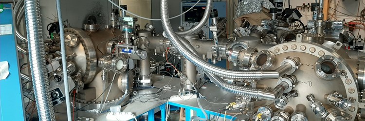
The MBE lab is a facility for epitaxial growth of layers and nanostructures based on III-V, II-VI and V-VI compounds
The MBE group runs a multi-chamber ultra-high vacuum system including:
• two twins Riber 32P molecular beam epitaxy growth chambers for III-V (AI, Ga, In)As andII-V-VI (Zn, Cd,Mn)(Bi, Sb)(Se, Te) semiconductor compounds;
• an analysis chamber for x-ray photoemission spectroscopy (XPS) equipped with a monochromatic Al Ka source (1486,7 eV) , overall resolution 0.9 eV;
• a chamber for the deposition of metals at room temperature.
The main research activity of the MBE group concentrates on semiconductor compound nanowires grown by molecular beam epitaxy.
Semiconductor nanowires are ideally 1-D nanostructures with diameter in the 10-100 nm range and in principle unconstrained length. Interest in these systems relies in the possibility they offer to exploit the properties related to their nano-scale size and their high surface to volume ratio in novel devices for electronics and optoelectronics.
Focus materials are III-V (GaAs, InAs, InGaAs) and II-VI (ZnSe, CdSe) compounds, and, very recently, on V2VI3topological insulator materials. The research activity concerns the understanding of the growth mechanism that leads to their highly anisotropic growth, the fabrication of radial (core/shell) or longitudinal nano-heterostructures, the growth of nanowire in homo- or hetero-epitaxial relationship with the substrate and of ordered array of identical wires, and the tuning of the nanowire electrical and magnetic properties by controlled incorporation of impurities.
We investigate the nanowire morphological, structural, optical and electronic properties, via scanning and transmission electron microscopy, Raman and photoluminescence spectroscopy, optical reflectivity, transport measurements and synchrotron radiation photoemission spectroscopy, in by house activity and thanks to collaborations.

