
Micro and nano patterning, with applications from biological sensors to micro devices.
The access to the facility is generally regulated by a commercial agreement, and is not subject to scientific evaluation. However FNF scientists will be happy to provide scientific advice to the users and are available for a deeper collaboration in those projects in which their scientific involvement could represent a further added value.
The access to private companies is limited to scientific research and prototype development. Any kind of production for commercial purposes is not admitted.
The users will be trained by the FNF staff to the use of the required equipment. Depending on the instrument and application complexity and on the previous experience of the user the training may last from one week up to one month. Eventually a habilitation (one for each piece of equipment) will be issued and the user will have free access to the instrumentation. The access will be subject to the temporal availability of the instruments and will be regulated through a proper booking system. The tool manager and the facility director can suspend the authorization of access and to require a new training in the event that the user is not considered independent in the laboratory processing.
The full FNF regulation can downloaded here.
Further information can be obtained at the facility web page
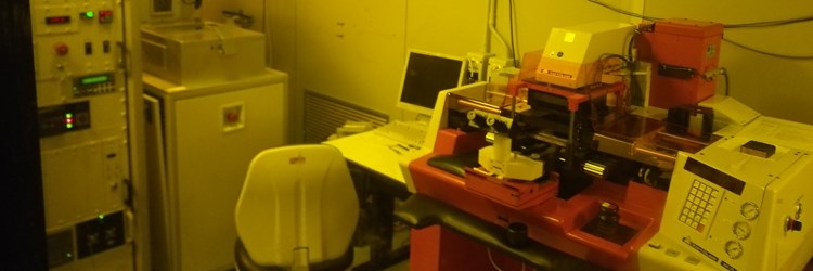
The FNF facility includes a wide range of instruments and tools allowing to complete the fabrication processes for the micro and nano fabrication. Most part of the instruments are hosted in 4 cleanrooms, ranging from class 10000 to 10. Four classes of instruments can be distinguished:
- patterning: UV lithography, nanoimprinting, UV interference lithography, cross beam equipped with external pattern generator for EBL like and direct FIB exposures;
- deposition tools: spin coaters, doctor blade, Sputtering, Thermal and e-gun evaporators, electroplating baths, PECVD, high temperature tubular oven for oxidation and thermal annealing;
- etching tools: wet etching hoods, RIE, ICP-DRIE;
- characterization: SEM, profilometers, light microscopes, contact angle setup, ellipsometer.
Thermal evaporator for highly controlled “glancing angle deposition” connected to nitrogen filled glove box, for application in stencil patterning and organic electronics. UV-NIL pneumatic press based on 254 nm flood exposure system. Homemade pneumatic press inserted in glove box for NIL processes requiring finely controlled environment (no water and oxygen presence). Fast NIL technology, able to imprint nanostructures in milliseconds. Systems for the growth of SAM for the tuning of surface properties of the materials.
The facility provides the tools and the expertise for the micro and nano patterning, in particular with top-down approach. The applications range from biological sensors, to high energy beam detectors, biological substrates, micro devices. Great effort is provided to the thin film growth by multiple approaches (PVD-CVD) for application in optics, mechanics, electronics. One of the main activities is the development and/or improvement of methodologies and techniques for micro and nano patterning, suitable for not conventional application.

