
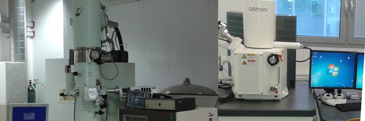
CEM is a center for electron microscopy for the analysis of nanostructured materials and methodological applications. It includes a TEM/STEM laboratory, a SEM facility and a sample preparation laboratory
The SEM microscope can be operated with 0.1-30kV acceleration voltage and a 4pA-10nA probe current with a nominal resolution of 1.3 nm at 15kV. It is equipped with a Everhart-Thornley Secondary Electron Detector, a High efficiency In-lens detector, this last providing an increased signal-to-noise ratio in image acquisition. A 10mm2 Oxford X-Act silicon drift detector for energy-dispersive x-ray spectroscopy (EDS) is annexed to the instrument, allowing to perform chemical analysis of the investigated samples.
A JEOL JEM 2010F UHR TEM/STEM is installed in a dedicated laboratory at TASC - MM building built by anchoring a concrete platform directly on the carsic rock with only weak links to the MM building. The TEM microscope has a thermally assisted field emission gun (FEG) electron source with a ZrO/W [100] filament. The high-brightness source produces a highly coherent electron probe with a diameter smaller than 0.13 nm and a resolution limit of 0.11 nm in phase contrast. The small probe size yields sub-nanometer resolution in analytical as well as spectroscopic measurements. The instrument is currently equipped with an 80mm2 Oxford X-Max silicon drift detector for EDS analysis allowing detection of light elements (Z > 5). The available scanning transmission electron microscopy (STEM) attachment coupled with EDS can be used to obtain chemical profiles with high spatial resolution. Moreover, coupling between the STEM attachment and the high-angle annular dark field (HAADF) detector is used to obtain Z-contrast imaging.
An intense research activity has been recently started on the development of a flow nanoreactor for in operando experiments by low voltage STEM and combined synchrotron spectroscopies. The device has been first conceived to be compatible with Grazing Incident Small Angle X-ray Scattering (GISAXS) and Wide-Angle X-ray Scattering (GIWAXS) where extended beam footprint (about 1x10 mm2) and small penetration of the beam are involved due to the grazing incidence geometry. The feasibility of our approach has been successfully demonstrated by monitoring shape and size evolution of PVP-capped Pd nanocrystals under oxidation/reaction conditions. Information on size, morphology of the nanocrystals obtained at the nanoscale by STEM have been coupled with that concerning their collective behaviour over extended areas such as size, aggregation and cristalline structure by GISAXS/GIWAXS, all in one portable microreactor and under identical reaction conditions. The research activity has been entirely carried out with the support of NFFA-Europe within the 30% in-house research quota reserved to CME, in strong synergy with the nanofabrication and synchrotron-based electronic characterization research groups operational at CNR-IOM. On-going projects include the study of nanocatalysts and nanoparticles for solar cell devices in reactive environments.
The research activity of the CME relies on the interconnected use of the TEM and SEM laboratories. In particular, the bulk of the research activity involves the characterization by TEM/STEM of the nanostructure and study of the interfacial properties of thin film heterostructures based on strongly correlated materials. On-going projects include the study of the role of substrate induced strain and defects on nanostructures of thin films.
In particular, material systems under investigation are perovskite oxides (e.g. TiO2, La0.7Sr0.3MnO3,…), transition metal dichalcogenides (e.g. MoS2, WSe2 …) and topological insulators (e.g. Bi2Se3, Bi2Te3, …) grown at the PLD-NFFA and Oxide MBE. Samples are first screened and investigated by SEM/EDS. TEM specimens are then prepared in different geometries (plan-view and cross-section) by mechanical polishing and further explored at atomic level by TEM/STEM to determine the relationships between structural, functional and electronic properties.
All experiments are supported by image simulation and data analysis treatment of the results obtained both in imaging and diffraction mode. The work is carried out in strong synergy with the growth and synchrotron-based electronic characterization research groups operational at CNR-IOM within and with the support of the NFFA research infrastructure projects aiming at continuously developing and operating an integrated users access infrastructure to nano-foundry services (growth, characterization, theory, fine analysis, FAIR data management), using dedicated resources from national and European grants, under the responsibility and coordination of Giorgio Rossi (UniMi and IOM-CNR).
Perspectives: a new Precision Ion Polishing System will be acquired in the coming months permitting to obtain higher quality TEM specimens by gentle mill at lower energies and at grazing incidence of solid state materials. Moreover, the catalytic experiments will benefit from the acquisition of a dedicated in-situ holder for TEM to perform experiments in different environments.

