The design and synthesis of materials with well-defined properties and functionalities is today one of the greatest challenges in the field of materials physics research. The new emerging class of two-dimensional (2D) materials, together with layered materials and all their possible combinations in hetero-structures, offers an ideal platform for the creation of systems with specific properties. 2D materials are defined as crystalline materials consisting of a single layer of atoms, while layered materials are compounds in which a crystal is built by stacking “two-dimensional” layers. The first 2D material ever isolated is graphene, a semimetal, in 2004. It consists of a single layer of sp2-bonded carbon atoms arranged in a honeycomb lattice, simply one single atomic layer of graphite. After graphene, a variety of different 2D materials emerged, displaying metallic (NbSe2, …), semiconducting (MoS2,… ) and insulating (hBN, …) character. Due to the confinement to one or few atomic layers, the properties of 2D materials can completely differ from their corresponding bulk crystals and can be further tuned in hybrid structures, where they are combined in vertical stacks, or when hetero-species are introduced in the lattice. The production of these new materials paves the way to a variety of important technological applications in, for example, photovoltaics, electronics, optoelectronics and mechanics.

The effective production of 2D and layered materials and of their heterostructures with designed functionalities requires a complex approach that combines the use of state-of-the-art growth techniques and advanced electronic and morphological characterization, as well as theoretical modeling for the prediction of the most appropriate material/system suitable for a specific application.
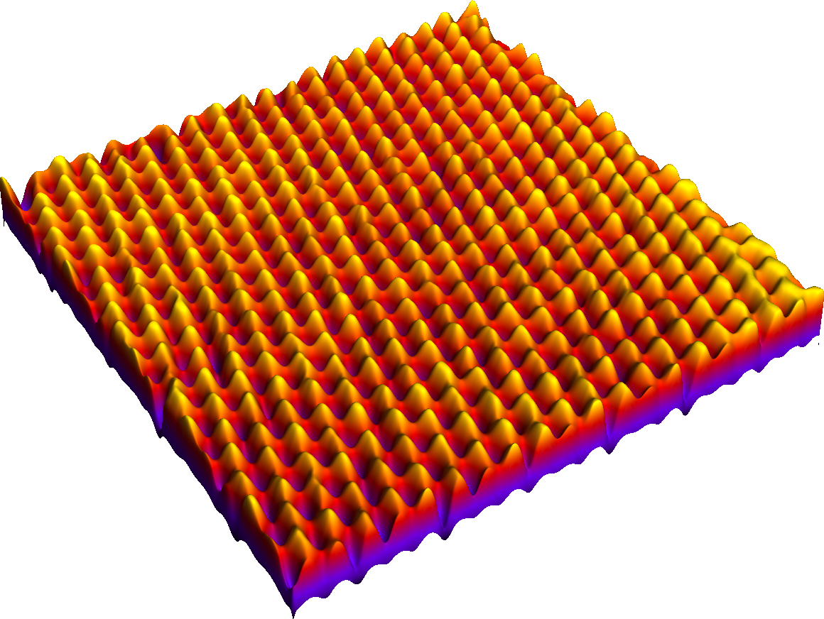
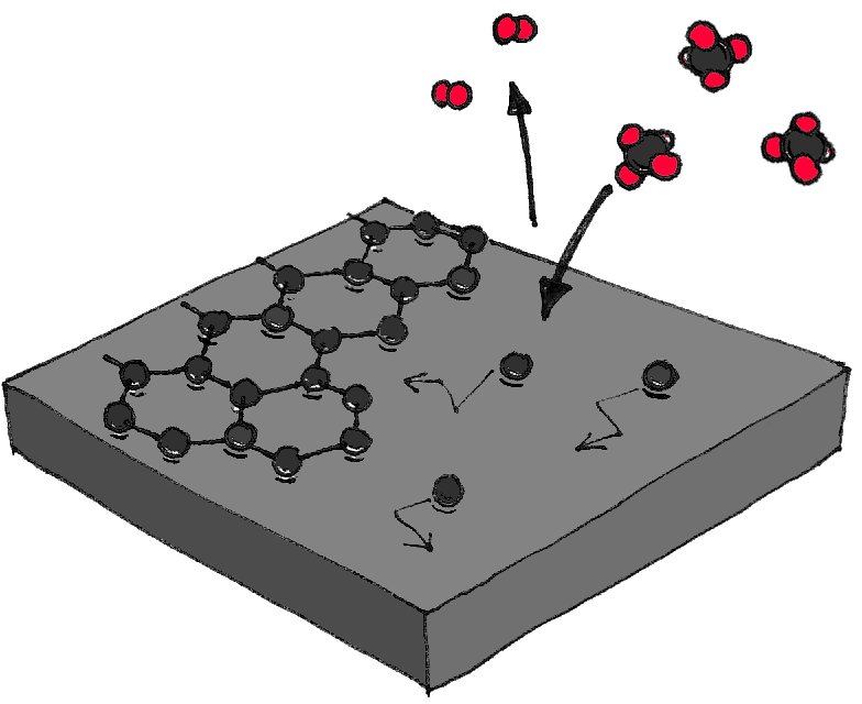
Several groups at IOM are active in this research area. The availability of state of the art synthesis setups, advanced electronic and morphological characterization techniques as well as cutting-edge theoretical calculations, allows IOM scientists to successfully grow, characterize and model many systems in this new class of materials, including graphene, h-BN, borophene, phosphorene, MoS2, PtSe2, GaSe, InSe, 2D layered/hybrid perovskites and 2D metal organic frameworks. Many routes are used to modulate/tailor their electronic properties, through, for example, doping, functionalization, deposition/growth on proper surfaces, as well as the creation of complex hetero-structures. Morphological and structural characterization down to the atomic level are achieved by means of advanced microscopy (STM, TEM, SEM), while a wide portfolio of spectroscopic techniques is used for the investigation of their electronic structure (both filled and empty states), vibrational modes and chemical reactivity, also using synchrotron radiation. Theoretical modeling focuses on many fundamental properties relevant for practical applications, including electronic, vibrational, thermal, optoelectronic, tribological properties, in- and out of- equilibrium.